Hardware that is checked before it is built.
Design review, board design, firmware testing and EMC pre-compliance, all done with our own in-house toolchain: every board is simulated, run against its own firmware and screened before it goes to the fab.
- 48 h design review turnaround, fixed price
- 68 firmware assertions passing in the emulator against the Paper Calendar’s circuit
- 4 field solvers of our own: cross-sections, power planes, return currents, 3D full wave
- 5 microcontroller families emulated, each core checked against QEMU
Four ways we take risk out of your board.
Design review in 48 hours
A second pair of eyes on your schematic and layout, with the datasheets open.
Send us your KiCad project, or the schematic and Gerbers. Within 48 hours you get a written review of the schematic, the layout and an EMC pre-compliance pass. Every finding names the part, the pin or the board location, cites the datasheet line it rests on and says how to fix it. The price is fixed and agreed before we start.
Talk about your board- Schematic checked against the datasheets: pin functions, ratings, strap pins, supply sequencing
- Layout checked for power paths, return paths, decoupling, fab rules and assembly
- EMC pre-compliance screening with located findings
- A written report with coordinates and a fix for each finding
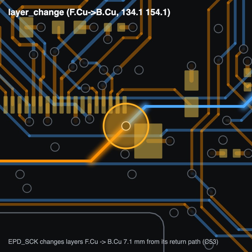
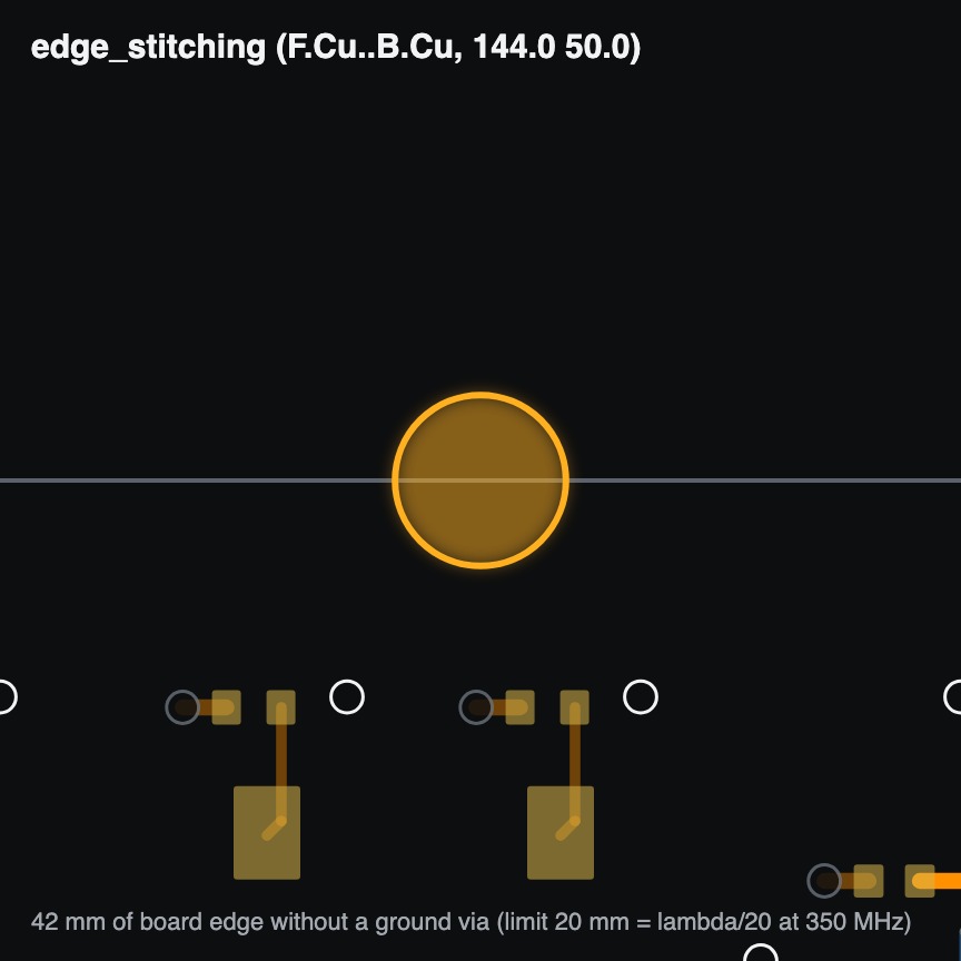
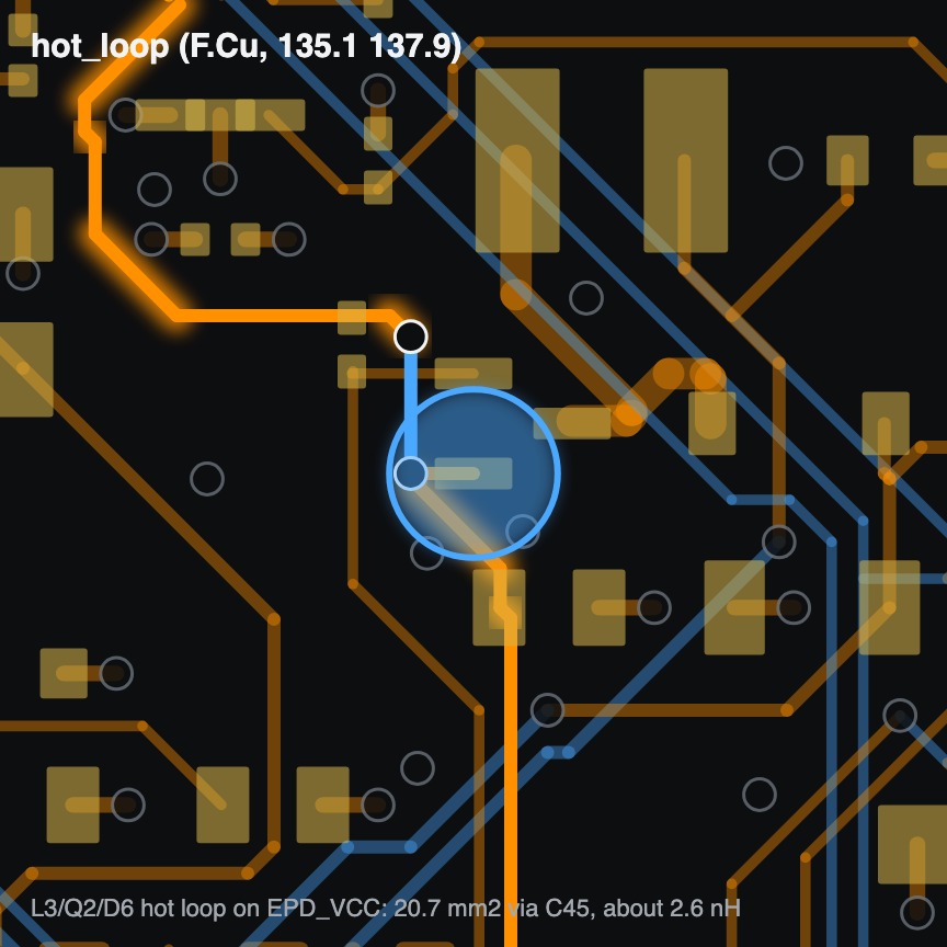
Proof On the Paper Calendar the EMC pass found 6 warnings on a board that already had no errors, each with its coordinates and a fix.
-
-
-
Idea to orderable board
From a requirements description to files you can send to the fab.
Describe what the board has to do. We turn it into a verified design: a schematic with checked parts, a routed layout and fabrication files designed to order with the fab’s standard options, so nothing special has to be explained to the fab. Prototypes can come assembled.
Talk about your board- ERC and DRC clean, with schematic and board proven to match
- Design-for-manufacture checks against JLCPCB’s capabilities
- EMC screening before release
- Gerbers, BOM and placement files, with parts picked from what is in stock
- An assembled prototype delivered to you
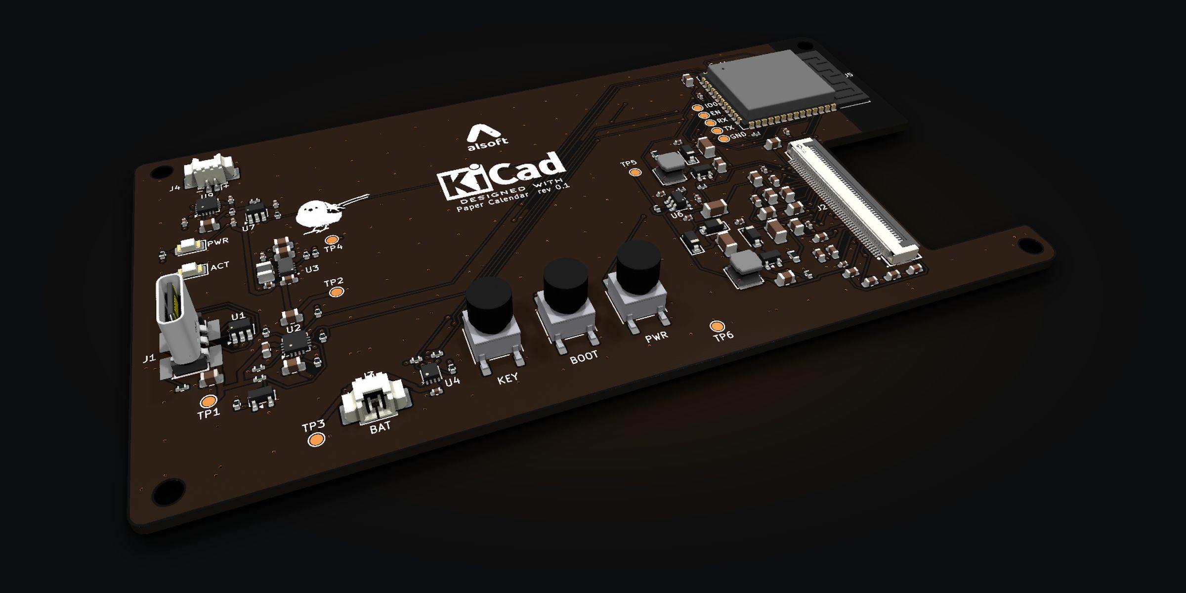
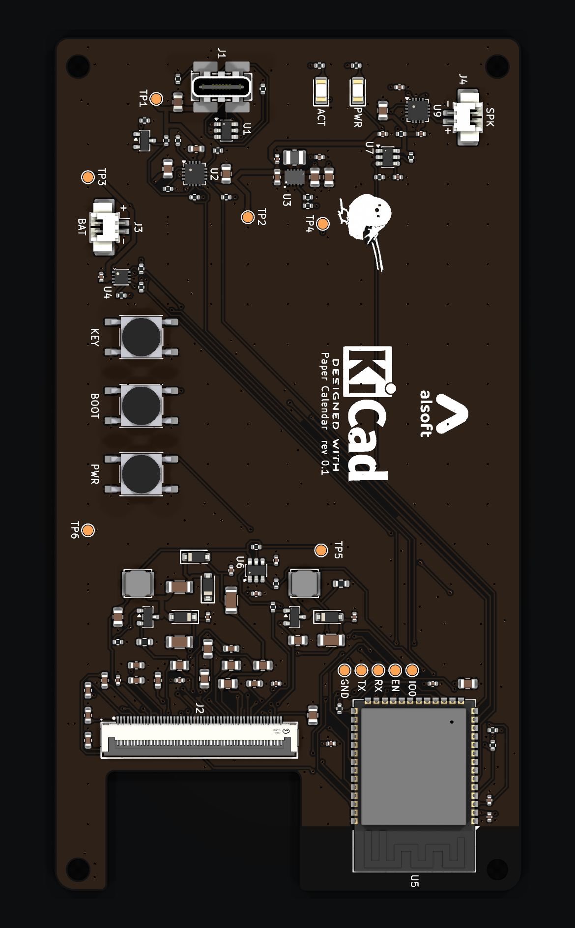
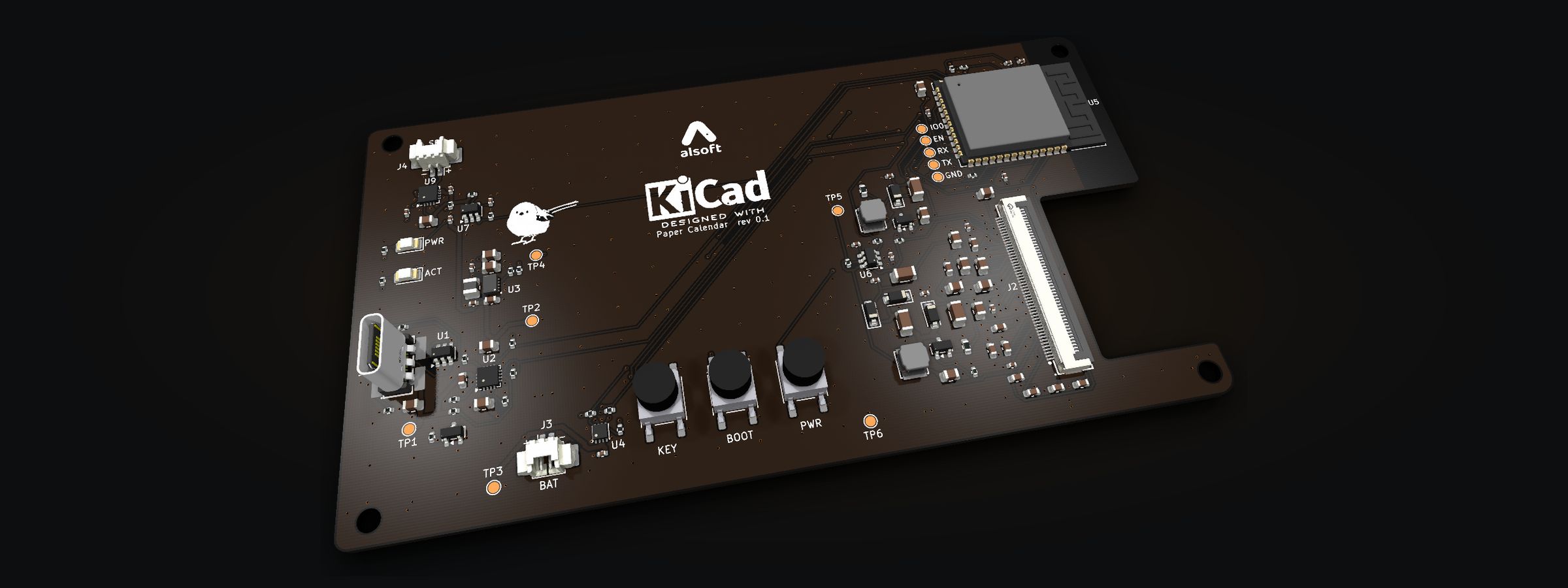
Proof The Paper Calendar: a 4-layer ESP32-S3 board with a 50-pin e-paper connector, charger, fuel gauge and audio amplifier, in manufacturing at JLCPCB since October 2026.
Firmware tested before the board exists
Your real firmware, running against your circuit, weeks before boards arrive.
Our emulator runs the firmware image you will flash on a model of the microcontroller, wired to a model of your board built from its circuit: pull-ups, buttons, regulators, fuel gauge, display controller. Scripted scenarios press buttons, drain the battery, cut the network or let days pass, and assert what the pins, buses, console and display did. Each CPU core is checked instruction by instruction against QEMU.
Talk about your board- ESP32-S3 and ESP32-C3, RP2040, i.MX RT1024 with Ethernet, AVR
- Scenarios for power, buttons, network and display
- Pixel-exact checks of what the display shows
- Runs headless, so it becomes a check in your CI
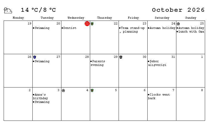
Proof The Paper Calendar’s production firmware boots end to end in the emulator: 7 scenarios and 68 assertions pass, including the exact image on the e-paper.
I (51) cpu_start: Multicore app
I (114) app_init: Project name:     paper-calendar
I (225) main_task: Calling app_main()
I (235) STATE: No remembered state (first boot or power loss)
I (275) NETWORK: Wi-Fi Started, calling connect...
I (2465) NETWORK: Got IP: 192.168.1.57
I (2875) NETWORK: Got time: 2026-10-21
I (4055) NETWORK: Got 10 calendar dates
I (7595) NETWORK: Got weather, Min: 8, Max: 14, Code: 7
I (7595) APP: Redrawing display
I (7625) POWER: Enabled display power
I (28285) POWER: Disabled display power
I (28285) APP: Sleeping for 602 seconds (timer 602000 ms, sleep timer 0 ppm)
first_boot: 14 assertions passed, 0 findings
EMC, SI and PI pre-compliance
Find what the compliance lab would find, while a fix is still cheap.
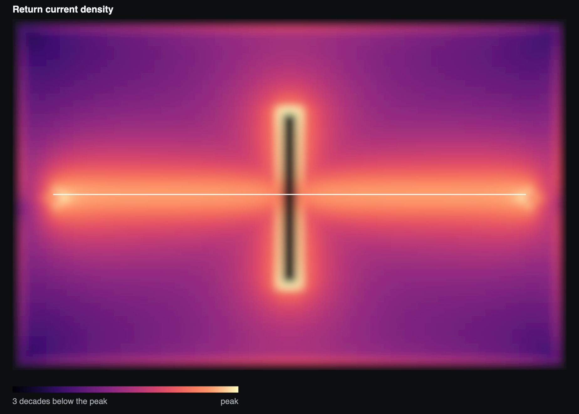
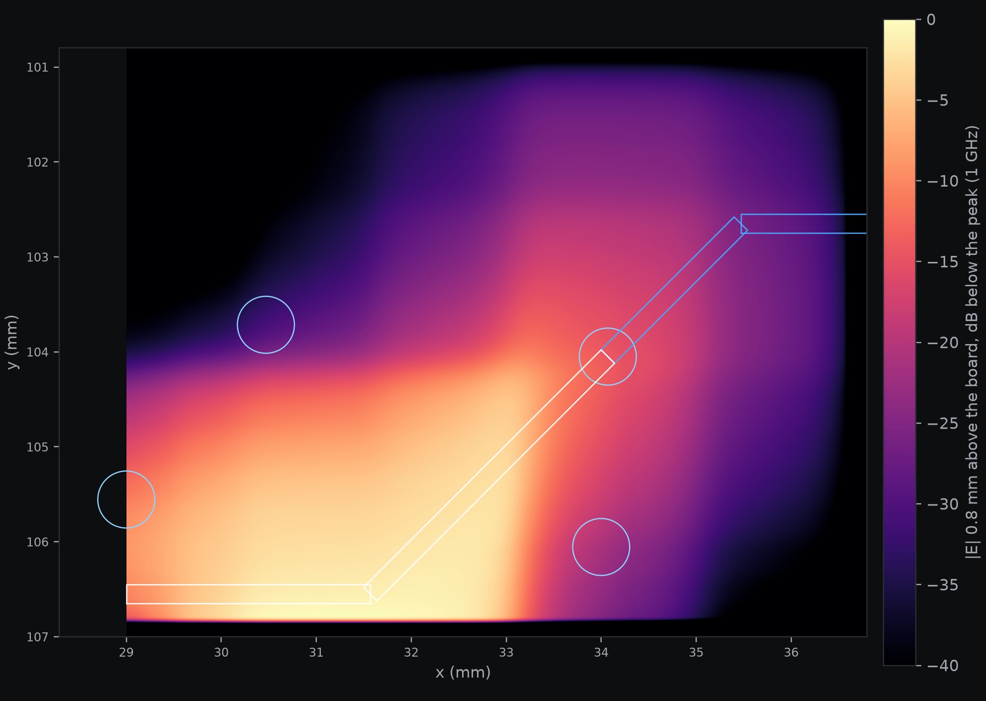
Our own field solvers, written for circuit boards, look at what rules of thumb miss: 2D cross-sections for impedance and crosstalk, the impedance of a power plane pair with your real decoupling capacitors, return current around slots and plane gaps, and a GPU 3D full-wave solver for the critical regions. Findings come with exact locations and fixes. These are pre-compliance estimates that reduce the risk of a lab visit. They are not certification.
Talk about your board- Trace impedance and crosstalk from the real stackup
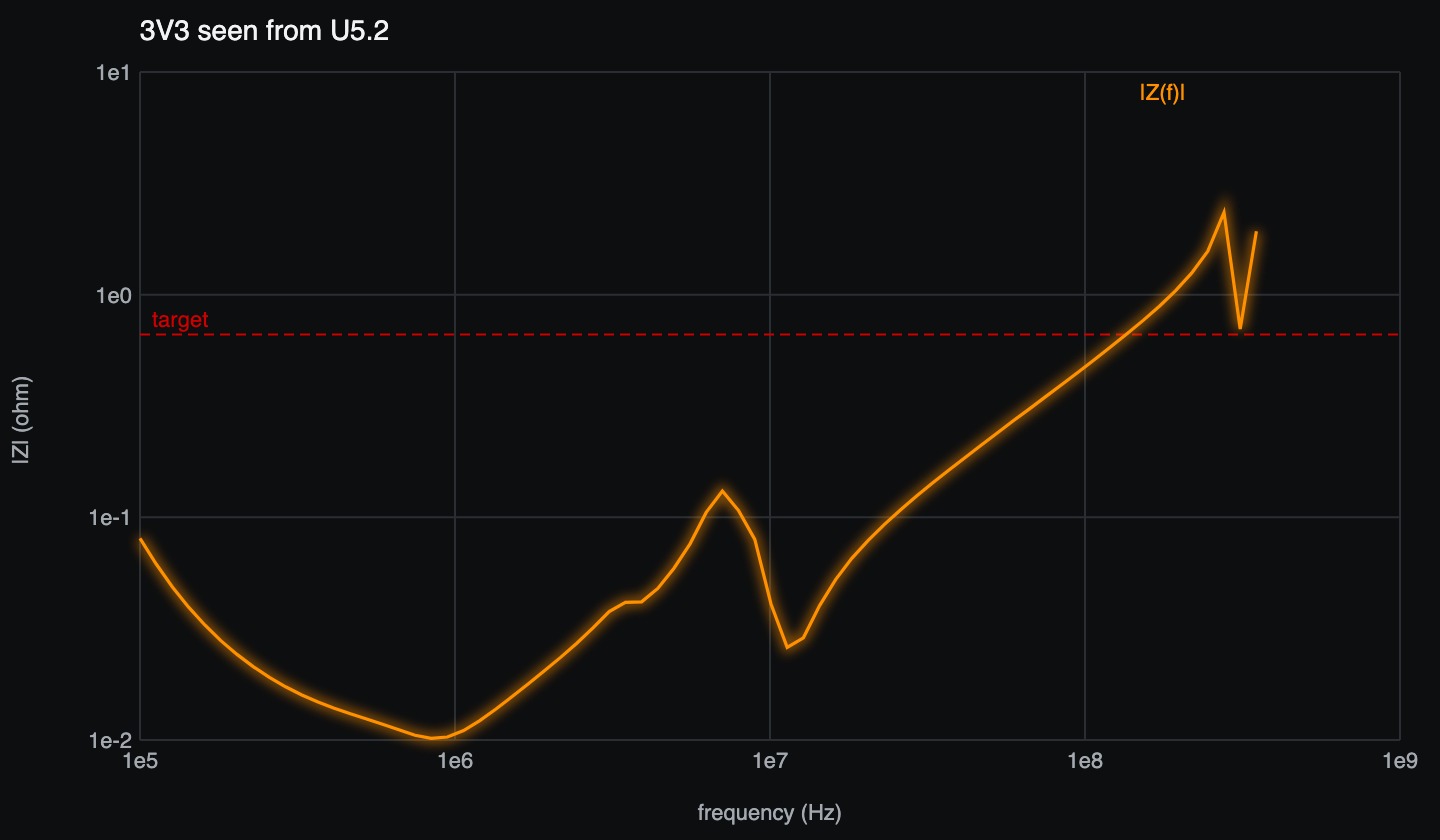
- Power-network impedance against a target, with the capacitors you placed
- Return current and the loop inductance a slot adds
- 3D full-wave fields for the regions that matter
Proof Measured against references: single traces within 0.3 % of the textbook formulas, stripline within 0.001 % of the exact solution, plane resonances within 0.06 % of the analytic cavity. On differential pairs with real copper it showed that the common closed-form formula reads 4 to 13 % low, confirmed with openEMS.
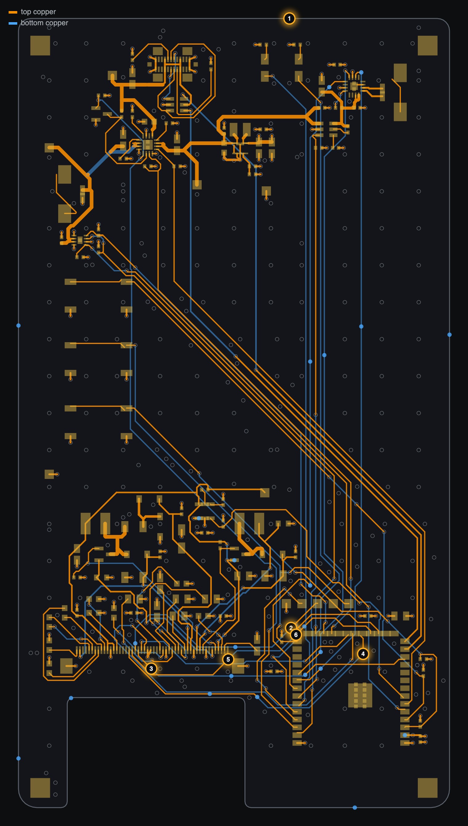
The whole board, screened.
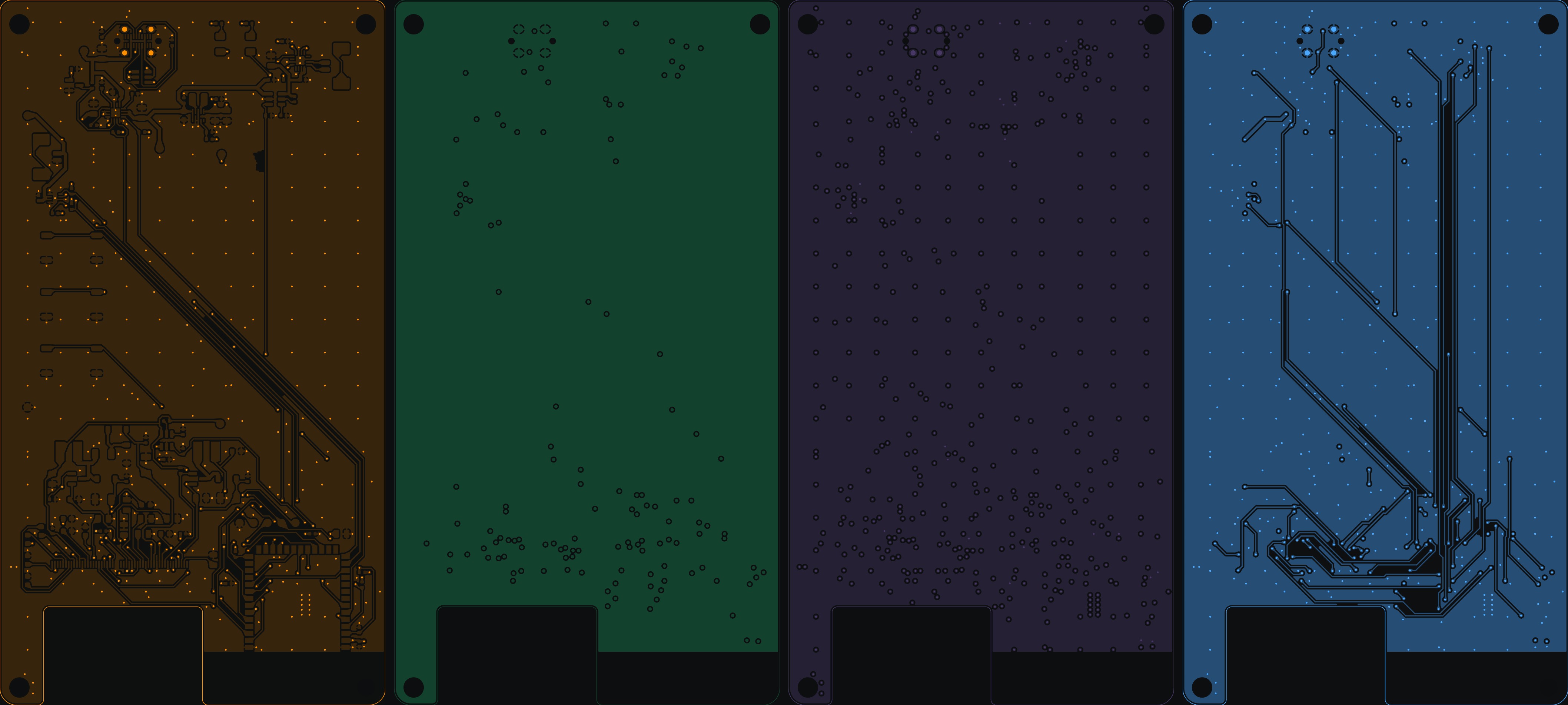
The EMC screen of the Paper Calendar on its real copper: six numbered warnings and 23 information items, each at its coordinates. Nothing is a guess about “the board”: every finding points at a place you can open in your layout tool.
- Warning
- Information
- Top copper
- Bottom copper
The Paper Calendar
Our own e-paper calendar: ESP32-S3, 4 layers, in manufacturing at JLCPCB.
We built it with the toolchain we use for customers, so we know what it finds and what it misses. The design came out of our checks with no errors. Its firmware runs end to end in the emulator against its own circuit. Its EMC screen then found what a normal review would not look for.
- 4 copper layers
- 7 / 68 scenarios / assertions passing in the emulator
- 6 EMC warnings, each with coordinates and a fix
What the EMC screen found
- Five vias where the e-paper SPI lines change layer are 6.2 to 9.5 mm from the nearest stitching capacitor (limit 3 mm at a 1 ns edge). Fix: a 100 nF capacitor within 3 mm of each, or one routing layer.
- 42 mm of the top edge has no ground via. Fix: two or three ground vias.
- The 3V3 plane impedance first exceeds its 0.66 ohm target at 136 MHz at the ESP32-S3, where the module’s own decoupling takes over.
Checked and fine
- No fast net crosses a gap in its reference plane
- Every supply pin has its capacitor within 5 mm
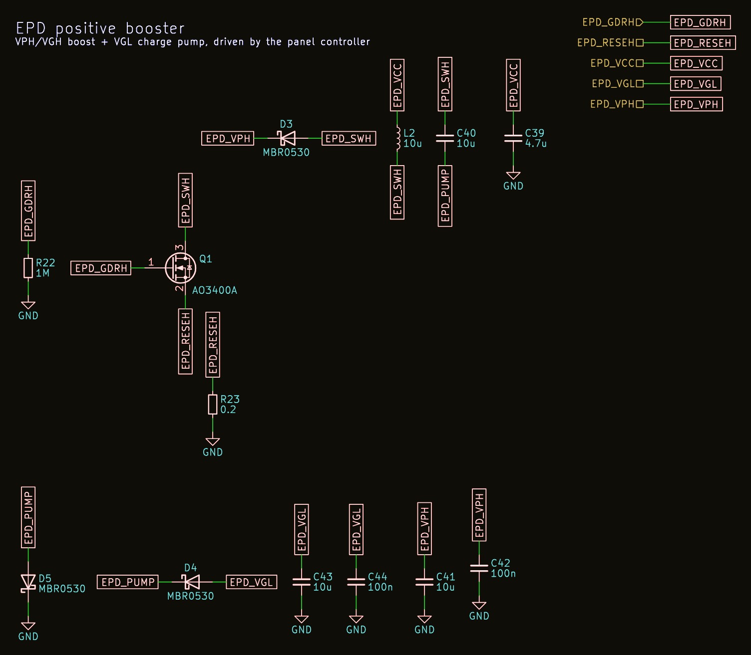
- The e-paper booster loops are about 2.6 nH and return in the plane
The warnings assume a 1 ns edge, the screen’s floor. Measuring the real edge on the first boards settles them, and that is how we hand findings over: what is known, what is assumed and how to settle it.
Simple, fixed and written down.
- 01
Chat
A short call about your board, your deadline and what worries you.
- 02
Fixed price
A written scope and a fixed price before any work starts.
- 03
Build and verify
Review, design, emulation or field solving, with every result traceable to a check.
- 04
Hand over
A report or the design files, with locations and fixes, and a call to walk through them.
Have a board to review, or an idea to build?
Tell us what you are making and when you need it. We reply within one business day.
Start a conversation